Abstract
Chip-off examination remains the method of last resort in digital forensics, applied when a device is locked, damaged or non-responsive, and it is the only route to data on many embedded targets such as vehicle event recorders and dashcams. The dominant removal technique is thermal reflow at approximately 360°C, and this is destructive to the evidence it recovers: charge leakage from flash memory is Arrhenius in temperature, so two minutes at 250°C consumes retention equivalent to centuries of room-temperature storage. This work develops a lower-temperature alternative using a consumer-grade 455 nm diode laser costing a small fraction of industrial equipment, together with an open-source browser-based tool that predicts thermal behaviour and gates recipes against two independent safety limits: wire-bond intermetallic damage and charge-retention loss. A finite element campaign in COMSOL Multiphysics characterised an eMMC package under a six-pass recipe. Two structural findings emerged. The bond-plane bulk temperature proved independent of remaining encapsulant thickness, because in quasi-steady state all absorbed power crosses the bond plane at fixed loop height regardless of the cap above it, which places the entire pass-to-pass risk in the per-pulse transient. Resolving finite spot size rather than assuming a one-dimensional heat source changed the predicted bond temperature from 181 to 272°C, which would condemn the process, to 94 to 139°C, which clears it. The campaign also identified two compensating errors in the tool's own analytical gate, which was corrected against the simulation. A single bench measurement, of laser spot size, returned 0.08 mm and satisfied a criterion recorded in advance. The wider bench validation programme is specified in full but was not executed, so the thermal model retains unverified status and all thermal figures reported are predictions rather than measurements. The claim advanced is one of data preservation, which is independent of encryption because charge leakage flips physical cells regardless of their contents.
Keywords
Digital Forensics, Chip-off, Laser Decapsulation, Epoxy Moulding Compound, NAND Flash, Data Retention,
Thermal Modelling, Finite Element Analysis
1. Introduction
Mobile device acquisition is conventionally tiered, progressing from logical extraction through file-system and physical acquisition to invasive methods
| [1] | Ayers, R., Brothers, S., Jansen, W. Guidelines on Mobile Device Forensics. NIST Special Publication 800-101 Revision 1. Gaithersburg, MD: National Institute of Standards and Technology; 2014. https://doi.org/10.6028/NIST.SP.800-101r1 |
[1]
. Chip-off sits at the invasive end: the memory device is physically removed from its board and read directly, bypassing the host controller and any software-level protection. It is used when a device is locked, non-responsive or physically damaged, and for embedded targets such as vehicle event recorders, dashcams and drones it is frequently the only route to the data
| [2] | Avanoz, T., Akbal, E. Data Recovery Application from NAND Flash Memories Using the Chip-Off Technique in Digital Forensics. International Journal of Innovative Engineering Applications. 2025, 9(2), 233-242.
https://doi.org/10.46460/ijiea.1797801 |
[2]
.
The dominant removal technique is thermal, heating the package until its solder reflows at working temperatures around 360°C
| [3] | Song, S., Yang, H., Lee, E., Lee, S., Kim, G. Forensic Recovery via Chip-Transplantation in Samsung Smartphones. Forensic Science International: Digital Investigation. 2025, 53, 301926. https://doi.org/10.1016/j.fsidi.2025.301926 |
[3]
. Its cost is borne by the evidence. Fukami et al. established that charge leakage from flash memory follows an Arrhenius relationship with an activation energy near 1.1 eV, such that two minutes at 250°C produces ageing equivalent to approximately 833 years of room-temperature retention, with raw bit-error rates rising by 38 to 432 times depending on prior wear
| [4] | Fukami, A., Ghose, S., Luo, Y., Cai, Y., Mutlu, O. Improving the Reliability of Chip-Off Forensic Analysis of NAND Flash Memory Devices. Digital Investigation. 2017, 20, S1-S11. https://doi.org/10.1016/j.diin.2017.01.011 |
[4]
. The damage is invisible to inspection: the die is intact and the device may still respond, but the stored data has been degraded by the act of recovering it.
Laser decapsulation offers a lower-temperature route and is established practice in failure analysis rather than a novel proposal. Dobriyal et al. place it among the routine options available to a failure-analysis laboratory
| [5] | Dobriyal, P., Kurella, A., Southwick, S. On-Board Package Decapsulation Techniques for Failure Analysis. In Proceedings of SMTA International, Rosemont, IL, 27 September–1 October 2015; pp. 117-121. |
[5]
, Anderson patented raster-scanned ablation to a selected depth
| [6] | Anderson, G. T. Failure Analysis Methods and Systems. US Patent 7, 271, 012 B2; 2007. |
[6]
, Carter documented the practical process window on transfer-moulded packages
| [7] | Carter, G. Laser Decapsulation of Transfer Molded Plastic Packages for Failure Analysis. In Proceedings of the 28th International Symposium for Testing and Failure Analysis (ISTFA 2002), Phoenix, AZ, 3–7 November 2002; pp. 117-125. https://doi.org/10.31399/asm.cp.istfa2002p0117 |
[7]
, and Aubert et al. reported in-process thermal monitoring during laser decapsulation
| [8] | Aubert, A., Dantas de Morais, L., Rebrassé, J.-P. Laser Decapsulation of Plastic Packages for Failure Analysis: Process Control and Artefact Investigations. Microelectronics Reliability. 2008, 48(8-9), 1144-1148. https://doi.org/10.1016/j.microrel.2008.07.004 |
[8]
. The equipment used in that literature is industrial, however, costing several thousand pounds and placing the technique beyond many publicly funded laboratories.
Two problems follow. First, accessibility: cost and operator skill concentrate the capability in a small number of practitioners, creating a single point of failure when a trained examiner is unavailable
| [9] | Mohammadi Anaei, M. T., Maniscalco, M., Choi, H., Roser, W., Emanuel, M., Phoulady, A., Mahyari, P., Blagojevic, A., May, N., Egan, G. C., Shahbazmohamadi, S., Tavousi, P. Integrated Femtosecond-Laser Workflow for Decapsulation, Delayering, and Cross-Sectioning of Advanced Package-on-Package Devices. Scientific Reports. 2026, 16(1), 25286.
https://doi.org/10.1038/s41598-026-56063-x |
[9]
. Second, and more fundamental, the existing literature does not characterise the process at the wavelength and in the thermal regime a low-cost diode laser occupies. Published ablation constants for epoxy derive from femtosecond ultraviolet work on unfilled resin
| [10] | Lu, M., Zhang, M., Zhang, K., Meng, Q., Zhang, X. Femtosecond UV Laser Ablation Characteristics of Polymers Used as the Matrix of Astronautic Composite Material. Materials. 2022, 15(19), 6771. https://doi.org/10.3390/ma15196771 |
[10]
, the only material-matched study uses femtosecond pulses at 800 nm
| [11] | Zhang, S., Shin, Y. C. Analysis of Ultrafast Laser Ablation of Fused Silica Filled EMC Using Improved Two Temperature Model. Journal of Manufacturing Processes. 2025, 141, 481-493. https://doi.org/10.1016/j.jmapro.2025.02.081 |
[11]
, and the closest methodological analogue works at microsecond timescales on unfilled polymers
| [12] | Kappes, R. S., Schönfeld, F., Li, C., Golriz, A. A., Nagel, M., Lippert, T., Butt, H.-J., Gutmann, J. S. A Study of Photothermal Laser Ablation of Various Polymers on Microsecond Time Scales. SpringerPlus. 2014, 3, 489.
https://doi.org/10.1186/2193-1801-3-489 |
[12]
. No source matches the combination of 455 nm wavelength, millisecond dwell and filler-dominated pigmented compound.
Table 1 summarises the principal decapsulation routes against the criteria that bear on forensic use, including the validation status of each.
Table 1. Comparison of decapsulation techniques by wavelength, operating temperature, target material, advantages, limitations and validation status.
Technique | Wavelength | Operating temperature | Material | Advantages | Limitations | Validation status |
Thermal reflow (chip-off) | n/a | Approx. 360°C | [3] | Song, S., Yang, H., Lee, E., Lee, S., Kim, G. Forensic Recovery via Chip-Transplantation in Samsung Smartphones. Forensic Science International: Digital Investigation. 2025, 53, 301926. https://doi.org/10.1016/j.fsidi.2025.301926 |
[3] | All moulded packages | Simple; low cost; widely practised | Arrhenius charge loss; two minutes at 250°C costs approx. 833 equivalent years | [4] | Fukami, A., Ghose, S., Luo, Y., Cai, Y., Mutlu, O. Improving the Reliability of Chip-Off Forensic Analysis of NAND Flash Memory Devices. Digital Investigation. 2017, 20, S1-S11. https://doi.org/10.1016/j.diin.2017.01.011 |
[4] | Established in casework; retention damage quantified | [4] | Fukami, A., Ghose, S., Luo, Y., Cai, Y., Mutlu, O. Improving the Reliability of Chip-Off Forensic Analysis of NAND Flash Memory Devices. Digital Investigation. 2017, 20, S1-S11. https://doi.org/10.1016/j.diin.2017.01.011 |
[4] |
Chemical (acid) etch | n/a | Approx. 60°C acid bath | [13] | Manoharan, S., Patel, C., McCluskey, F. P., Pecht, M. G. Effective Decapsulation of Copper Wire-Bonded Microelectronic Devices for Reliability Assessment. Microelectronics Reliability. 2018, 84, 197-207.
https://doi.org/10.1016/j.microrel.2018.03.028 |
[13] | Epoxy; gold bonds | Selective; preserves gold bonds | Attacks copper; fume handling; trained operator | [5] | Dobriyal, P., Kurella, A., Southwick, S. On-Board Package Decapsulation Techniques for Failure Analysis. In Proceedings of SMTA International, Rosemont, IL, 27 September–1 October 2015; pp. 117-121. | | [13] | Manoharan, S., Patel, C., McCluskey, F. P., Pecht, M. G. Effective Decapsulation of Copper Wire-Bonded Microelectronic Devices for Reliability Assessment. Microelectronics Reliability. 2018, 84, 197-207.
https://doi.org/10.1016/j.microrel.2018.03.028 |
[5, 13] | Established in failure analysis | [13] | Manoharan, S., Patel, C., McCluskey, F. P., Pecht, M. G. Effective Decapsulation of Copper Wire-Bonded Microelectronic Devices for Reliability Assessment. Microelectronics Reliability. 2018, 84, 197-207.
https://doi.org/10.1016/j.microrel.2018.03.028 |
[13] |
Plasma or chemical finish | n/a | Not reported | Epoxy residue | Non-contact; clears residual layer | Impractical for bulk removal; a finishing stage only | [8] | Aubert, A., Dantas de Morais, L., Rebrassé, J.-P. Laser Decapsulation of Plastic Packages for Failure Analysis: Process Control and Artefact Investigations. Microelectronics Reliability. 2008, 48(8-9), 1144-1148. https://doi.org/10.1016/j.microrel.2008.07.004 |
[8] | Established as a finishing stage | [8] | Aubert, A., Dantas de Morais, L., Rebrassé, J.-P. Laser Decapsulation of Plastic Packages for Failure Analysis: Process Control and Artefact Investigations. Microelectronics Reliability. 2008, 48(8-9), 1144-1148. https://doi.org/10.1016/j.microrel.2008.07.004 |
[8] |
Industrial infrared laser | 1064 nm | Localised; not reported | Transfer-moulded epoxy | Copper reflects approx. 95%, sparing the bonds | [6] | Anderson, G. T. Failure Analysis Methods and Systems. US Patent 7, 271, 012 B2; 2007. | | [22] | Zhou, J., Xia, G., Zhou, Z., Chen, C., Long, Y. Comparison Study of 6082 Al Alloy Laser Welding Using 455 nm Blue Laser and 1080 nm Near-Infrared Laser. Optik. 2022, 272, 170224. https://doi.org/10.1016/j.ijleo.2022.170224 |
[6, 22] | Capital cost of several thousand pounds | Established in failure analysis | [6] | Anderson, G. T. Failure Analysis Methods and Systems. US Patent 7, 271, 012 B2; 2007. | | [7] | Carter, G. Laser Decapsulation of Transfer Molded Plastic Packages for Failure Analysis. In Proceedings of the 28th International Symposium for Testing and Failure Analysis (ISTFA 2002), Phoenix, AZ, 3–7 November 2002; pp. 117-125. https://doi.org/10.31399/asm.cp.istfa2002p0117 |
[6, 7] |
Femtosecond laser | 800 nm | [11] | Zhang, S., Shin, Y. C. Analysis of Ultrafast Laser Ablation of Fused Silica Filled EMC Using Improved Two Temperature Model. Journal of Manufacturing Processes. 2025, 141, 481-493. https://doi.org/10.1016/j.jmapro.2025.02.081 |
[11] | [10] | Lu, M., Zhang, M., Zhang, K., Meng, Q., Zhang, X. Femtosecond UV Laser Ablation Characteristics of Polymers Used as the Matrix of Astronautic Composite Material. Materials. 2022, 15(19), 6771. https://doi.org/10.3390/ma15196771 |
[10] | Athermal; minimal heat-affected zone | Filled EMC | [11] | Zhang, S., Shin, Y. C. Analysis of Ultrafast Laser Ablation of Fused Silica Filled EMC Using Improved Two Temperature Model. Journal of Manufacturing Processes. 2025, 141, 481-493. https://doi.org/10.1016/j.jmapro.2025.02.081 |
[11] | [10] | Lu, M., Zhang, M., Zhang, K., Meng, Q., Zhang, X. Femtosecond UV Laser Ablation Characteristics of Polymers Used as the Matrix of Astronautic Composite Material. Materials. 2022, 15(19), 6771. https://doi.org/10.3390/ma15196771 |
[10] | Minimal thermal damage | High capital cost; published constants derive from unfilled resin | [10] | Lu, M., Zhang, M., Zhang, K., Meng, Q., Zhang, X. Femtosecond UV Laser Ablation Characteristics of Polymers Used as the Matrix of Astronautic Composite Material. Materials. 2022, 15(19), 6771. https://doi.org/10.3390/ma15196771 |
[10] | Characterised for filled EMC | [11] | Zhang, S., Shin, Y. C. Analysis of Ultrafast Laser Ablation of Fused Silica Filled EMC Using Improved Two Temperature Model. Journal of Manufacturing Processes. 2025, 141, 481-493. https://doi.org/10.1016/j.jmapro.2025.02.081 |
[11] |
Microsecond-pulse laser | 810 nm | [12] | Kappes, R. S., Schönfeld, F., Li, C., Golriz, A. A., Nagel, M., Lippert, T., Butt, H.-J., Gutmann, J. S. A Study of Photothermal Laser Ablation of Various Polymers on Microsecond Time Scales. SpringerPlus. 2014, 3, 489.
https://doi.org/10.1186/2193-1801-3-489 |
[12] | Photothermal; not reported | Unfilled polymers | [12] | Kappes, R. S., Schönfeld, F., Li, C., Golriz, A. A., Nagel, M., Lippert, T., Butt, H.-J., Gutmann, J. S. A Study of Photothermal Laser Ablation of Various Polymers on Microsecond Time Scales. SpringerPlus. 2014, 3, 489.
https://doi.org/10.1186/2193-1801-3-489 |
[12] | Closest published thermal analogue | Not filler-dominated; not 455 nm | [12] | Kappes, R. S., Schönfeld, F., Li, C., Golriz, A. A., Nagel, M., Lippert, T., Butt, H.-J., Gutmann, J. S. A Study of Photothermal Laser Ablation of Various Polymers on Microsecond Time Scales. SpringerPlus. 2014, 3, 489.
https://doi.org/10.1186/2193-1801-3-489 |
[12] | Characterised for unfilled polymers | [12] | Kappes, R. S., Schönfeld, F., Li, C., Golriz, A. A., Nagel, M., Lippert, T., Butt, H.-J., Gutmann, J. S. A Study of Photothermal Laser Ablation of Various Polymers on Microsecond Time Scales. SpringerPlus. 2014, 3, 489.
https://doi.org/10.1186/2193-1801-3-489 |
[12] |
This work | 455 nm | Approx. 73°C bulk; bond peak below 150°C (both predicted) | Filled, pigmented black EMC | Consumer-grade cost; two independent safety gates | Absorptivity assumed rather than measured; needs a chemical or plasma finish | Unverified: simulation-based, with one measured parameter (spot size) |
This work addresses both. It develops a decapsulation methodology for wire-bonded eMMC, NAND and NOR memory packages using a consumer-grade 455 nm diode laser, supported by an open-source browser-based tool that predicts thermal behaviour and enforces two independent safety gates. It reports a finite element campaign characterising the process, and it specifies in full the empirical validation programme required before the method can be used on evidence.
The claim advanced is specifically one of data preservation, meaning that the stored charge survives the process, and this is measurable at cell level regardless of whether the contents are encrypted. Recovery, meaning the interpretation of surviving bits, is a separate problem addressed by other techniques and is not claimed here.
2. Materials and Methods
2.1. Target Devices and Materials
Test vehicles are wire-bonded eMMC, NAND and NOR memory packages, dead or unprogrammed, drawn from the same production lot where possible. The method applies only to packages whose interconnect sits above the die beneath the mould cap. Flip-chip constructions are excluded by geometry rather than convenience, since the safety criterion used here is the encapsulant remaining over the wire loop, and that quantity has no referent where bumps sit beneath an inverted die.
The baseline encapsulant is black epoxy moulding compound, modelled with thermal conductivity 0.8 W m-1 K-1, density 1850 kg m-3, specific heat 1000 J kg-1 K-1 and absorptivity 0.95 at 455 nm. The provenance of these values differs and the distinction is material. The thermal properties fall within the range reported for filled compounds in memory packaging, whose composition is characterised as 60 to 80% inorganic filler by weight, 5 to 20% resin and under 1% carbon black
| [13] | Manoharan, S., Patel, C., McCluskey, F. P., Pecht, M. G. Effective Decapsulation of Copper Wire-Bonded Microelectronic Devices for Reliability Assessment. Microelectronics Reliability. 2018, 84, 197-207.
https://doi.org/10.1016/j.microrel.2018.03.028 |
[13]
. The absorptivity value is not literature-derived: no measurement of black moulding compound absorptance at 455 nm exists in the open literature, and 0.95 is an assumed default. It is therefore carried as a declared uncertainty rather than a measured input, and direct measurement of moulding compound absorptance at 455 nm is identified in Section 4.6 as a high-value validation activity.
That absence matters because the method depends on the pigment rather than the polymer. Neat epoxy resin has an absorption edge near 3.06 eV, approximately 405 nm
| [14] | Durmuş, H., Şafak, H., Akbaş, H. Z., Ahmetli, G. Optical Properties of Modified Epoxy Resin with Various Oxime Derivatives in the UV-VIS Spectral Region. Journal of Applied Polymer Science. 2011, 120(3), 1490-1495.
https://doi.org/10.1002/app.33287 |
[14]
, so at 455 nm it is below its band edge and only weakly absorbing, and it remains weakly absorbing through the near-infrared
| [15] | Blass, D., Dilger, K., Nyga, S., Jungbluth, B., Hoffmann, H.-D. Composite Bonding Pre-Treatment with Laser Radiation of 3 µm Wavelength. Materials. 2018, 11(7), 1216.
https://doi.org/10.3390/ma11071216 |
[15]
. Absorption at the working wavelength is therefore extrinsic, arising from the carbon black, which is consistent with the finding that filled compound must be modelled using carbon's optical properties rather than a weighted average of its constituents
| [11] | Zhang, S., Shin, Y. C. Analysis of Ultrafast Laser Ablation of Fused Silica Filled EMC Using Improved Two Temperature Model. Journal of Manufacturing Processes. 2025, 141, 481-493. https://doi.org/10.1016/j.jmapro.2025.02.081 |
[11]
.
Bond metallurgy determines the temperature limit. Post-2015 devices predominantly use 30 µm copper wire, gated here at 150°C on the copper-aluminium intermetallic growth kinetics measured by Hang et al. on copper ball bonds on aluminium metallisation in green moulding compound
| [16] | Hang, C. J., Wang, C. Q., Mayer, M., Tian, Y. H., Zhou, Y., Wang, H. H. Growth Behavior of Cu/Al Intermetallic Compounds and Cracks in Copper Ball Bonds During Isothermal Aging. Microelectronics Reliability. 2008, 48(3), 416-424. https://doi.org/10.1016/j.microrel.2007.06.008 |
[16]
. Because the mechanism is diffusion-controlled, this is applied as a conservative time-at-temperature limit rather than a sharp threshold.
2.2. Laser System and Configuration
The source is a Sculpfun iCube 3W diode laser emitting at 455 nm under GRBL firmware control. Three configuration requirements are enforced.
GRBL laser mode is disabled by setting the $32 parameter to zero. With it enabled the firmware suppresses spindle on and off commands during motion, silently converting the intended time-domain pulse train into continuous-wave output and invalidating any prediction made for a pulsed regime.
The regime is millisecond thermal pulsing, not nanosecond ablative pulsing. Pulse durations are 15 to 100 ms, peak power equals average power, removal proceeds by thermochemical decomposition rather than plasma-mediated ablation, and the heat-affected zone is of order 50 to 200 µm. The benefit claimed for pulsing is thermal relaxation between pulses, not cold ablation.
Air assist is treated as a safety constraint. The model assumes a 3.5 m/s jet giving a convective coefficient of 110 W m-2 K-1, derived from the machine specification of 15 litres per minute using the Blasius-Pohlhausen laminar flat-plate correlation
| [17] | Bergman, T. L., Lavine, A. S., Incropera, F. P., DeWitt, D. P. Fundamentals of Heat and Mass Transfer. 7th ed. Hoboken, NJ: Wiley; 2011. |
[17]
. The correlation assumes parallel flow, so a genuinely impinging jet would give a higher coefficient, making the value conservative with respect to cooling.
Spot size is measured rather than assumed. Because fluence scales with the inverse of spot area, an error in this parameter propagates into every fluence-dependent quantity. The measurement procedure requires three independent stationary bursts at confirmed focal height with both axes measured and a standard deviation below 5 µm.
2.3. Thermal Model
The model gates on two independent failure modes and is biased toward stopping early where a constant is uncertain.
The first gate addresses wire-bond integrity. Bond temperature is decomposed as a bulk soak plus a per-pulse increment. The per-pulse term is derived from ablation-front conduction
| [18] | Carslaw, H. S., Jaeger, J. C. Conduction of Heat in Solids. 2nd ed. Oxford: Oxford University Press; 1959. |
[18]
, in which the irradiated surface is held at the ablation temperature and heat conducts past that front to the bond plane:
Tbond = T0 + (Tabl − T0) · erfc(ξ), ξ = z / (2√(αt)) (1)
where
T0 is the accumulated bulk soak rather than ambient,
z is the standoff, α the thermal diffusivity and
t the pulse duration. Inverting equation (
1) for the depth at which
Tbond reaches the metallurgical limit yields the minimum safe standoff, which is the model's actionable output.
Two corrections to this form were required and are reported in Section 3. Evaluating the error function at the end of the pulse under-reads the peak, because the bond-plane maximum lags the pulse end; the Duhamel peak of the finite pulse is used instead. And the one-dimensional form assumes an infinite heated area, ignoring lateral spreading.
The second gate addresses data retention. Bond survival is not data survival, since the memory array experiences the bulk soak for the entire recipe. An Arrhenius charge-leakage constraint is evaluated separately, expressing the acceleration factor relative to a 25°C reference:
AF = exp[(Ea / k) · (1/Tref − 1/T)](2)
with
Ea taken as 1.1 eV
| [4] | Fukami, A., Ghose, S., Luo, Y., Cai, Y., Mutlu, O. Improving the Reliability of Chip-Off Forensic Analysis of NAND Flash Memory Devices. Digital Investigation. 2017, 20, S1-S11. https://doi.org/10.1016/j.diin.2017.01.011 |
[4]
. The output is the retention margin remaining after processing, expressed in equivalent-25°C years, which converts an abstract multiplier into a read-back window.
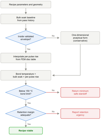
Figure 1. Dual-gate safety architecture.
Ablation depth uses the logarithmic law standard in laser processing
, with the effective ablation enthalpy as the consumed constant. The direction-of-error asymmetry is load-bearing: overstating this constant causes the model to believe each pass removes less material than it does, authorising passes after the real front has reached the keep-out, whereas understating it merely leaves excess encapsulant.
The relationship between the two gates and the recipe verdict is shown in
Figure 1. The two gates are evaluated independently. Outside the envelope for which finite element data exists, the gate falls back to the one-dimensional analytical form, which is never less conservative than the interpolated value, so leaving the validated region can only tighten the constraint.
2.4. Finite Element Model
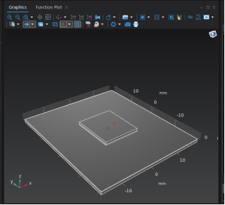
Simulation was performed in COMSOL Multiphysics 6.4 with the Heat Transfer and Structural Mechanics modules. Package geometry was generated from datasheet dimensions as watertight non-overlapping solids, one per structural element (mould compound, silicon die, bond wires, bond pads, substrate, solder balls and board), and imported using Form Assembly with pair creation enabled, resolving to 158 domains for the probe model and 174 for the finalised model carrying representative bond wires. The assembled geometry is shown in
Figure 2.
Figure 2. Assembled package and board geometry prior to meshing, with the bond-plane point probe at the die corner.
The moulding compound carries temperature-dependent conductivity and specific heat, a char layer at the ablation front and a decomposition energy sink. Air-assist convection is applied to the top and side faces, with an explicit heat-sink condition on the underside; omitting either produces monotonic runaway rather than a plausible but wrong answer, which is a useful diagnostic property.
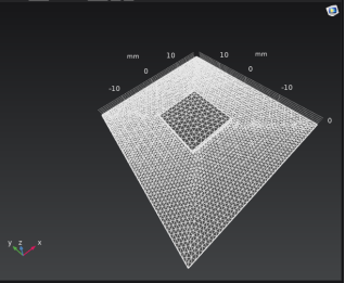
The discretisation is shown in
Figure 3. Free tetrahedral meshing was applied with local refinement over the die region, where the through-thickness gradient is steepest, and a coarser distribution across the surrounding board, giving 862,029 elements and approximately 1.6 million degrees of freedom.
The moving spot is implemented as an averaged-power surface heat flux masked to the die footprint. Heat input is verified by surface integration before any temperature is read, and this verification is repeated once the boundary begins to deform, because the irradiated area is then no longer constant. Material removal uses a Deformed Geometry interface applied to the mould domain alone at 0.015 mm per pass.
Figure 3. Finite element mesh of the package and board assembly, with local refinement over the die footprint. Axes are in millimetres.
Because simulating every pulse is infeasible, the per-pulse contribution is resolved in a separate axisymmetric cell in which the irradiated surface is pinned at the ablation temperature through a penalty-flux condition. A gated Dirichlet condition was rejected because it clamps the surface back to ambient once the pulse ends, actively refrigerating the spot and biasing the post-pulse bond peak low. The cell is run well beyond the pulse length, since the bond-plane peak arrives after the pulse ends, and the reported quantity is the peak rather than the end-of-pulse value.
2.5. Software Implementation and Verification
The tool is a single HTML file released under AGPLv3 with no server component and no network requests, so it can be run from a local copy on an air-gapped workstation and its source can be examined by an opposing expert. It computes the gates described above, generates machine instructions, and stamps each generated file with the model version, its physical basis, the predicted margins and a cryptographic fingerprint of the parameter set.
Verification comprises two automated suites. A unit suite of 600 tests exercises the physics and analysis layers, executed against source extracted programmatically from the shipped file rather than a transcribed copy, so that a passing run is evidence about the artefact itself. A separate end-to-end suite covers interface-dependent paths. Statement coverage of the wire-bond gate is 99.3% with branch coverage 91.8%; the single uncovered statement is provably unreachable.
2.6. Validation Strategy
Model status is declared on a three-point ladder. Unverified indicates no experimental data; calibrated indicates correction factors applied from measurement; validated requires predictions within 10% of measured values together with satisfaction of repeatability criteria. Both conditions are required for the last, since accuracy without repeatability does not qualify.
Pre-calibration expectations were set deliberately low to prevent over-interpretation: 15 to 25% for single-pass surface temperature and 20 to 30% for multi-pass bond temperature, limited by absorptivity uncertainty and assumed bond loop height respectively.
3. Results
3.1. Model Verification
Before any temperature was read, delivered heat input was verified by surface integration over the irradiated face. The model injects 0.39501 W within every scan window and exactly zero in every inter-pass cooling gap, and this figure is constant across all six passes, confirming that the deforming ablation boundary does not alter the injected power.
3.2. Bond-Plane Thermal Behaviour
The bulk temperature at the bond plane does not rise as the encapsulant above it thins. Predicted values across the six-pass recipe were 73.5, 72.5, 72.5, 72.7, 72.9 and 73.0°C.
The reason is structural rather than numerical. In quasi-steady state all absorbed power must pass through the bond plane en route from the surface to the die and out through the substrate and solder balls. The bond plane sits at a fixed loop height above the die, so the temperature drop between bond and die is set by that fixed distance and the through-flux, an expression in which the cap thickness above the bond plane does not appear. Thinning the cap lowers the surface temperature relative to the die and leaves the bond-to-die drop untouched.
The consequence is that risk does not accumulate gradually as processing proceeds. It resides entirely in the transient of each individual pulse.
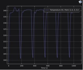
The corresponding die-top trace is shown in
Figure 4. Each pass reaches a plateau near 340 K, and the inter-pass intervals return the die to within a few kelvin of its starting condition, so no pass begins from a materially elevated baseline. The absence of an upward drift across the six passes is the same behaviour observed at the bond plane and is the direct evidence for the structural argument above.
Figure 4. Predicted die-top temperature against process time across the six-pass recipe.
The bulk term scales linearly with laser power, with a simulated temperature-rise ratio of 1.656 against an ideal 1.667, an error of 0.6%. This conclusion is conditional on adequate cooling. A single-variable run with the air jet removed, reducing top convection from 110 to 8 W m-2 K-1, drove the bulk to 342°C and still climbing, with inter-pass gaps never resetting. Air assist is therefore a hard safety constraint rather than a quality preference.
3.3. Per-Pulse Contribution and Finite-Spot Correction
The capped unit cell gives a per-pulse rise of 63 K at the bond plane, with the peak arriving approximately 9 ms after the 15 ms pulse ends.
A 28-run finite-spot sweep is the decisive result. A one-dimensional plane treatment places the bonds at 181 to 272°C, condemning the six-pass recipe; however, resolving lateral spreading with a disc source clears the issue.
Table 2. Predicted worst-case bond peak temperature (°C) for a single pulse from the 73°C bulk soak, by standoff and effective spot diameter. All realistic-spot cases fall below the 150°C copper limit. Values are finite element predictions, not physical measurements.
Standoff (mm) | 0.08 mm spot | 0.12 mm spot | 0.15 mm spot | Plane (1-D) |
0.130 | 109.7 | 126.8 | 138.6 | 214 |
0.145 | 101.9 | 116.1 | 126.3 | 203 |
0.160 | 96.1 | 107.9 | 116.6 | 193 |
0.175 | 91.7 | 101.5 | 108.9 | 185 |
0.190 | 88.2 | 96.5 | 102.8 | 177 |
0.205 | 85.5 | 92.5 | 97.9 | 170 |
0.220 | 83.4 | 89.3 | 94.0 | 163 |
The same data is charted in
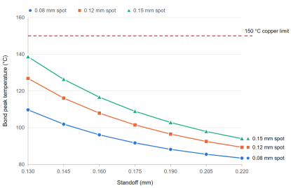
Figure 5, which makes the two governing behaviours visible at a glance: the strong dependence on spot diameter at fixed standoff, and the comfortable clearance of every realistic-spot case below the 150°C limit. All three series remain below that limit across the swept range, and the one-dimensional plane predictions of
Table 2 lie above the scale shown.
Figure 5. Predicted bond peak temperature against standoff for effective spot diameters of 0.08 mm (circles), 0.12 mm (squares) and 0.15 mm (triangles).
Every realistic-spot case is predicted to fall below the limit. At the measured spot of 0.08 mm the worst case across the swept standoffs reaches 109.7°C against a 150°C limit, a margin of 40°C. Had the spot measured 0.15 mm the same case would have reached 138.6°C, a margin of 11.4°C. These are model predictions: no bond temperature has been measured, so the margins quoted are predicted margins rather than demonstrated ones.
All 28 transient peaks lie below their analytical steady-state disc ceilings, the surface pin held at its target throughout, and results are monotone in both depth and beam radius, providing three independent consistency checks.
3.4. Correction of the Analytical Gate
Comparison between the analytical gate and the finite element model revealed errors in both directions.
Table 3. Finite element plane-source temperature rise against the analytical prediction, showing a depth-dependent under-read.
Standoff (mm) | FEM plane rise (K) | Analytical rise (K) | Ratio |
0.130 | 141.3 | 121.5 | 1.16 |
0.160 | 120.2 | 88.7 | 1.36 |
0.190 | 104.4 | 66.1 | 1.58 |
0.220 | 89.5 | 50.6 | 1.77 |
The analytical form under-read the one-dimensional temperature rise by an average of 47%, worsening with depth, for two stacked reasons: its boundary formulation refrigerated the surface after each pulse, and it assumed constant rather than temperature-dependent properties. Simultaneously it omitted lateral spreading entirely, biasing it the other way. The two errors partially cancelled, leaving the tool net conservative, predicting 194.5°C where the finite element model gives 138.6°C, which is how it came to condemn a viable recipe. Neither error would have been visible from either model alone.
The correction applied was a direct interpolation table built from
Table 2 rather than a multiplicative factor. It reproduces the source data to 0.023°C across 21 verification points.
3.5. Spot Size Measurement
The burn test returned an effective spot of 0.08 mm, matching the manufacturer specification rather than the larger figure typical of mass-produced diode modules. This satisfies the criterion recorded before the measurement was taken and places the process in the most favourable series of
Figure 5.
3.6. Scope of the Results Obtained
The bench programme specified in Section 2.6 was not executed. One measurement was obtained, reported in Section 3.5; everything else reported here is finite element output.
The model therefore retains unverified status as the final status of this work. Specifically, this work does not claim that the tool predicts bond temperature correctly, that the 150°C limit has been shown sufficient in this regime, or that any encapsulant has been successfully removed from a physical package by this method.
4. Discussion
4.1. Interpretation of the Thermal Findings
Two results change how the process should be understood and modelled.
The standoff-independence of the bulk term is counter-intuitive and reframes what a safety gate is for. It is not tracking a slowly rising danger as material is removed; it is checking a repeated short event against a limit. That distinction matters for process design, because it implies inter-pass cooling controls the bulk term while pulse parameters control the risk.
The finite-spot correction is not a refinement of a broadly correct answer but the difference between a verdict of unsafe and one of safe with margin. Any thermal gate built on a one-dimensional assumption for a small spot will err in this specific direction, and will err conservatively, which is the failure mode least likely to be noticed and therefore most likely to persist.
A third observation generalises beyond this work. The original gate's error was not a wrong equation; the equation was correct. It was evaluated at the wrong time, at pulse end rather than at the lagging peak. Reviews of an expression will not catch that, because the expression checks out.
4.2. Comparison With Existing Methods
The incumbent technique operates at approximately 360°C
| [3] | Song, S., Yang, H., Lee, E., Lee, S., Kim, G. Forensic Recovery via Chip-Transplantation in Samsung Smartphones. Forensic Science International: Digital Investigation. 2025, 53, 301926. https://doi.org/10.1016/j.fsidi.2025.301926 |
[3]
against approximately 73°C predicted here. The significance of that gap is exponential rather than proportional, because the governing failure is Arrhenius. Two minutes at 250°C consumes roughly 833 years of equivalent retention
| [4] | Fukami, A., Ghose, S., Luo, Y., Cai, Y., Mutlu, O. Improving the Reliability of Chip-Off Forensic Analysis of NAND Flash Memory Devices. Digital Investigation. 2017, 20, S1-S11. https://doi.org/10.1016/j.diin.2017.01.011 |
[4]
; a process predicted to hold near 73°C for the duration of a decapsulation consumes retention measured in days.
This should not be overstated. Thermal chip-off does not always destroy data, which is why it remains standard practice. What the evidence shows is that it consumes retention budget at a rate making survival dependent on how much budget remained, so a lightly worn recently seized device tolerates it while a heavily worn device stored for two years may not. The laser process does not make recovery possible where it was impossible; it removes the temperature term from the risk.
Against chemical decapsulation the comparison differs in character. Acid etching preserves gold bonds but attacks copper, the dominant modern metallurgy, and requires fume handling and trained operators
| [5] | Dobriyal, P., Kurella, A., Southwick, S. On-Board Package Decapsulation Techniques for Failure Analysis. In Proceedings of SMTA International, Rosemont, IL, 27 September–1 October 2015; pp. 117-121. |
[5]
. The techniques are complementary rather than competing: laser ablation is a bulk-removal stage requiring a chemical or plasma finish
| [8] | Aubert, A., Dantas de Morais, L., Rebrassé, J.-P. Laser Decapsulation of Plastic Packages for Failure Analysis: Process Control and Artefact Investigations. Microelectronics Reliability. 2008, 48(8-9), 1144-1148. https://doi.org/10.1016/j.microrel.2008.07.004 |
[8]
.
A distinction the comparison depends upon is that preservation is not recovery. On modern handsets, memory contents are encrypted and bound to device hardware, so reading the memory in isolation yields ciphertext
| [3] | Song, S., Yang, H., Lee, E., Lee, S., Kim, G. Forensic Recovery via Chip-Transplantation in Samsung Smartphones. Forensic Science International: Digital Investigation. 2025, 53, 301926. https://doi.org/10.1016/j.fsidi.2025.301926 |
[3]
. The preservation claim holds regardless, because charge leakage flips physical cells whether or not their contents are ciphertext, but the practical value of the method concentrates on unencrypted and embedded targets.
4.3. Model Fidelity and Its Limits
Accuracy cannot be assessed without measurement. Fidelity, meaning whether the model represents the right physics, can be.
Cross-model comparison established that two errors partially cancelled, which is the most instructive fidelity result obtained. A single-model check would have reported a plausible answer, and a comparison of final verdicts would have shown agreement; only comparing intermediate quantities exposed both. Agreement between two models is weaker evidence than it appears.
Three sensitivities dominate. Spot size enters as an inverse square and propagates into every fluence-dependent quantity; it has now been measured. Mould cap thickness determines whether the true standoff falls within the range evaluated at all and remains datasheet-derived, making it the highest-value outstanding measurement. Absorptivity at 455 nm has never been measured for black moulding compound.
4.4. Failure Modes
Five failure modes are identifiable and they differ in visibility. Bond damage is modelled and detectable by inspection. Data loss without physical damage is invisible, and is the mode distinguishing forensic decapsulation from failure analysis. Incomplete decapsulation is recoverable, which is why the model is biased toward it.
Two are not represented in the model. Filler particles produce non-uniform ablation, with stalagmites where removal is marginal and micro-lensing where transparent particles focus the beam, so the real front has a depth distribution and the binding constraint is its deepest excursion rather than its mean
| [7] | Carter, G. Laser Decapsulation of Transfer Molded Plastic Packages for Failure Analysis. In Proceedings of the 28th International Symposium for Testing and Failure Analysis (ISTFA 2002), Phoenix, AZ, 3–7 November 2002; pp. 117-125. https://doi.org/10.31399/asm.cp.istfa2002p0117 |
[7]
.
Package alteration outside the intended one is also possible. Laser modification of cavity walls has been reported to create a parasitic conduction path that doubled a device’s reverse current while leaving the die undamaged
| [8] | Aubert, A., Dantas de Morais, L., Rebrassé, J.-P. Laser Decapsulation of Plastic Packages for Failure Analysis: Process Control and Artefact Investigations. Microelectronics Reliability. 2008, 48(8-9), 1144-1148. https://doi.org/10.1016/j.microrel.2008.07.004 |
[8]
. An examiner inspecting the die would have found nothing wrong.
4.5. Forensic Applicability
Decapsulation is irreversibly destructive, so the governing standard is not preservation of the exhibit but characterised alteration, under which a competent person must be able to explain and justify their actions
| [20] | Association of Chief Police Officers. ACPO Good Practice Guide for Digital Evidence. Version 5. London: ACPO; 2012. |
[20]
. The tool supports this by predicting exposure in advance, recording the prediction alongside the outcome, and hashing both into a tamper-evident record. Laboratories are additionally expected to validate methods within their own quality systems
| [21] | International Organization for Standardization. ISO/IEC 17025: 2017 General Requirements for the Competence of Testing and Calibration Laboratories. Geneva: ISO; 2017. |
[21]
, which this work specifies but does not perform.
The method also has dual-use character that should be stated rather than elided. Decapsulation is a prerequisite for invasive attack on integrated circuits, and cost reduction lowers the barrier for any actor. Three considerations bear on this: the capability is not novel, being mature and commercially available
| [6] | Anderson, G. T. Failure Analysis Methods and Systems. US Patent 7, 271, 012 B2; 2007. |
[6]
; what changes is cost; and the material presented concerns bulk removal and its thermal control rather than any attack methodology.
4.6. Limitations and Future Work
The principal limitation is that no thermal prediction has been checked against measurement, so the model is currently unverified. Executing the specified programme is the single change that would most alter what can be claimed and will be conducted at a later date.
Within it, three measurements carry disproportionate value: a cross-section to establish mould cap thickness and front roughness; a direct measurement of moulding compound absorptance at 455 nm; and determination of die-surface damage onset, which could be obtained by stepped hotplate exposure of sacrificial dies with metallisation imaged after each increment.
Three extensions follow from findings rather than omissions. Thermal-mechanical stress becomes the limiting failure mode once heat and charge retention are addressed and is presently neither modelled nor measured. Non-destructive determination of die position, for instance by scanning acoustic microscopy exploiting the acoustic impedance difference between compound and silicon, would remove the largest geometric uncertainty at source.
An infrared successor would address a boundary specific to the chosen wavelength. Copper reflects roughly 95% of 1064 nm light but absorbs on the order of 60% at 455 nm
| [22] | Zhou, J., Xia, G., Zhou, Z., Chen, C., Long, Y. Comparison Study of 6082 Al Alloy Laser Welding Using 455 nm Blue Laser and 1080 nm Near-Infrared Laser. Optik. 2022, 272, 170224. https://doi.org/10.1016/j.ijleo.2022.170224 |
| [23] | Nordet, G., Gorny, C., Mayi, Y., Daligault, J., Dal, M., Effernelli, A., Blanchet, E., Coste, F., Peyre, P. Absorptivity Measurements During Laser Powder Bed Fusion of Pure Copper with a 1 kW CW Green Laser. Optics and Laser Technology. 2022, 147, 107612.
https://doi.org/10.1016/j.optlastec.2021.107612 |
[22, 23]
, inverting the rationale for infrared decapsulation, in which copper reflectivity is precisely what spares the bonds
| [6] | Anderson, G. T. Failure Analysis Methods and Systems. US Patent 7, 271, 012 B2; 2007. |
[6]
. Full electrical exposure of the bonds is therefore unattainable at 455 nm, and the residual encapsulant functions as an optical shield as well as a thermal one.
5. Conclusions
This work developed a laser decapsulation methodology for wire-bonded memory packages using consumer-grade 455 nm hardware, supported by an open-source tool enforcing two independent safety gates. It is offered as a simulation-informed methodology and a specified validation framework rather than as a demonstrated casework technique.
Four contributions are offered. A quantified correction to how such a gate should be constructed, since a one-dimensional treatment of conducted bond temperature condemns a recipe that a finite-spot treatment clears, and the difference is entirely lateral heat spreading. A dual-gate architecture combining metallurgical and charge-retention limits, which follows from holding the failure-analysis and forensic literatures in view together, since neither produces the correct design alone. An auditable implementation in which every constant carries its provenance and the model declares its own validation status. And a specified validation programme with acceptance criteria fixed before any data existed.
A methodological outcome is also worth recording. The finite element campaign did not merely characterise the process; it corrected the software, identifying two compensating errors in the analytical gate that neither model would have revealed alone.
The principal limitation is equally clear. No thermal prediction has been validated against physical measurement, and the method should not be applied to irreplaceable evidence until that programme has been executed. The appropriate use of this work is as the basis for that programme rather than as a casework technique.
Abbreviations
ACPO | Association of Chief Police Officers |
BER | Bit–Error Rate |
CW | Continuous Wave |
EMC | Epoxy Moulding Compound |
FEM | Finite Element Method |
GRBL | Open–source Motion Control Firmware |
HTC | Heat Transfer Coefficient |
ISO | International Organization for Standardization |
NAND | Not–AND (flash Memory Type) |
NOR | Not–OR (flash Memory Type) |
eMMC | Embedded MultiMediaCard |
Author Contributions
George Lloyd: Conceptualization, Data curation, Formal Analysis, Investigation, Methodology, Project administration, Resources, Software, Supervision, Validation, Visualization, Writing – original draft, Writing – review & editing
Data Availability Statement
Two animations of the finite element solution are available as supplementary material include the Open-decap glitlab repo. The animations are referenced from Section 3.2: the heating and cooling cycle across the six-pass recipe, and the heating sequence of the cell-depth study. Neither is reproducible in print. The 28-run parametric sweep data underlying
Table 2 and
Figure 5 is also available in tabular form.
The data underlying this study are available from the author upon request.
Conflicts of Interest
The author declares no conflicts of interest.
References
| [1] |
Ayers, R., Brothers, S., Jansen, W. Guidelines on Mobile Device Forensics. NIST Special Publication 800-101 Revision 1. Gaithersburg, MD: National Institute of Standards and Technology; 2014.
https://doi.org/10.6028/NIST.SP.800-101r1
|
| [2] |
Avanoz, T., Akbal, E. Data Recovery Application from NAND Flash Memories Using the Chip-Off Technique in Digital Forensics. International Journal of Innovative Engineering Applications. 2025, 9(2), 233-242.
https://doi.org/10.46460/ijiea.1797801
|
| [3] |
Song, S., Yang, H., Lee, E., Lee, S., Kim, G. Forensic Recovery via Chip-Transplantation in Samsung Smartphones. Forensic Science International: Digital Investigation. 2025, 53, 301926.
https://doi.org/10.1016/j.fsidi.2025.301926
|
| [4] |
Fukami, A., Ghose, S., Luo, Y., Cai, Y., Mutlu, O. Improving the Reliability of Chip-Off Forensic Analysis of NAND Flash Memory Devices. Digital Investigation. 2017, 20, S1-S11.
https://doi.org/10.1016/j.diin.2017.01.011
|
| [5] |
Dobriyal, P., Kurella, A., Southwick, S. On-Board Package Decapsulation Techniques for Failure Analysis. In Proceedings of SMTA International, Rosemont, IL, 27 September–1 October 2015; pp. 117-121.
|
| [6] |
Anderson, G. T. Failure Analysis Methods and Systems. US Patent 7, 271, 012 B2; 2007.
|
| [7] |
Carter, G. Laser Decapsulation of Transfer Molded Plastic Packages for Failure Analysis. In Proceedings of the 28th International Symposium for Testing and Failure Analysis (ISTFA 2002), Phoenix, AZ, 3–7 November 2002; pp. 117-125.
https://doi.org/10.31399/asm.cp.istfa2002p0117
|
| [8] |
Aubert, A., Dantas de Morais, L., Rebrassé, J.-P. Laser Decapsulation of Plastic Packages for Failure Analysis: Process Control and Artefact Investigations. Microelectronics Reliability. 2008, 48(8-9), 1144-1148.
https://doi.org/10.1016/j.microrel.2008.07.004
|
| [9] |
Mohammadi Anaei, M. T., Maniscalco, M., Choi, H., Roser, W., Emanuel, M., Phoulady, A., Mahyari, P., Blagojevic, A., May, N., Egan, G. C., Shahbazmohamadi, S., Tavousi, P. Integrated Femtosecond-Laser Workflow for Decapsulation, Delayering, and Cross-Sectioning of Advanced Package-on-Package Devices. Scientific Reports. 2026, 16(1), 25286.
https://doi.org/10.1038/s41598-026-56063-x
|
| [10] |
Lu, M., Zhang, M., Zhang, K., Meng, Q., Zhang, X. Femtosecond UV Laser Ablation Characteristics of Polymers Used as the Matrix of Astronautic Composite Material. Materials. 2022, 15(19), 6771.
https://doi.org/10.3390/ma15196771
|
| [11] |
Zhang, S., Shin, Y. C. Analysis of Ultrafast Laser Ablation of Fused Silica Filled EMC Using Improved Two Temperature Model. Journal of Manufacturing Processes. 2025, 141, 481-493.
https://doi.org/10.1016/j.jmapro.2025.02.081
|
| [12] |
Kappes, R. S., Schönfeld, F., Li, C., Golriz, A. A., Nagel, M., Lippert, T., Butt, H.-J., Gutmann, J. S. A Study of Photothermal Laser Ablation of Various Polymers on Microsecond Time Scales. SpringerPlus. 2014, 3, 489.
https://doi.org/10.1186/2193-1801-3-489
|
| [13] |
Manoharan, S., Patel, C., McCluskey, F. P., Pecht, M. G. Effective Decapsulation of Copper Wire-Bonded Microelectronic Devices for Reliability Assessment. Microelectronics Reliability. 2018, 84, 197-207.
https://doi.org/10.1016/j.microrel.2018.03.028
|
| [14] |
Durmuş, H., Şafak, H., Akbaş, H. Z., Ahmetli, G. Optical Properties of Modified Epoxy Resin with Various Oxime Derivatives in the UV-VIS Spectral Region. Journal of Applied Polymer Science. 2011, 120(3), 1490-1495.
https://doi.org/10.1002/app.33287
|
| [15] |
Blass, D., Dilger, K., Nyga, S., Jungbluth, B., Hoffmann, H.-D. Composite Bonding Pre-Treatment with Laser Radiation of 3 µm Wavelength. Materials. 2018, 11(7), 1216.
https://doi.org/10.3390/ma11071216
|
| [16] |
Hang, C. J., Wang, C. Q., Mayer, M., Tian, Y. H., Zhou, Y., Wang, H. H. Growth Behavior of Cu/Al Intermetallic Compounds and Cracks in Copper Ball Bonds During Isothermal Aging. Microelectronics Reliability. 2008, 48(3), 416-424.
https://doi.org/10.1016/j.microrel.2007.06.008
|
| [17] |
Bergman, T. L., Lavine, A. S., Incropera, F. P., DeWitt, D. P. Fundamentals of Heat and Mass Transfer. 7th ed. Hoboken, NJ: Wiley; 2011.
|
| [18] |
Carslaw, H. S., Jaeger, J. C. Conduction of Heat in Solids. 2nd ed. Oxford: Oxford University Press; 1959.
|
| [19] |
Bäuerle, D. Laser Processing and Chemistry. 4th ed. Berlin: Springer; 2011.
https://doi.org/10.1007/978-3-642-17613-5
|
| [20] |
Association of Chief Police Officers. ACPO Good Practice Guide for Digital Evidence. Version 5. London: ACPO; 2012.
|
| [21] |
International Organization for Standardization. ISO/IEC 17025: 2017 General Requirements for the Competence of Testing and Calibration Laboratories. Geneva: ISO; 2017.
|
| [22] |
Zhou, J., Xia, G., Zhou, Z., Chen, C., Long, Y. Comparison Study of 6082 Al Alloy Laser Welding Using 455 nm Blue Laser and 1080 nm Near-Infrared Laser. Optik. 2022, 272, 170224.
https://doi.org/10.1016/j.ijleo.2022.170224
|
| [23] |
Nordet, G., Gorny, C., Mayi, Y., Daligault, J., Dal, M., Effernelli, A., Blanchet, E., Coste, F., Peyre, P. Absorptivity Measurements During Laser Powder Bed Fusion of Pure Copper with a 1 kW CW Green Laser. Optics and Laser Technology. 2022, 147, 107612.
https://doi.org/10.1016/j.optlastec.2021.107612
|
Cite This Article
-
APA Style
Lloyd, G. (2026). Low-Cost Laser Decapsulation of Wire-Bonded Memory Packages with Dual Thermal Gating for Forensic Data Preservation. American Journal of Mechanical and Industrial Engineering, 11(5), 113-123. https://doi.org/10.11648/j.ajmie.20261105.12
 Copy
|
Copy
|
 Download
ACS Style
Lloyd, G. Low-Cost Laser Decapsulation of Wire-Bonded Memory Packages with Dual Thermal Gating for Forensic Data Preservation. Am. J. Mech. Ind. Eng. 2026, 11(5), 113-123. doi: 10.11648/j.ajmie.20261105.12
Copy
|
Download
AMA Style
Lloyd G. Low-Cost Laser Decapsulation of Wire-Bonded Memory Packages with Dual Thermal Gating for Forensic Data Preservation. Am J Mech Ind Eng. 2026;11(5):113-123. doi: 10.11648/j.ajmie.20261105.12
Copy
|
Download
-
@article{10.11648/j.ajmie.20261105.12,
  author = {George Lloyd},
  title = {Low-Cost Laser Decapsulation of Wire-Bonded Memory Packages with Dual Thermal Gating for Forensic Data Preservation},
  journal = {American Journal of Mechanical and Industrial Engineering},
  volume = {11},
  number = {5},
  pages = {113-123},
  doi = {10.11648/j.ajmie.20261105.12},
  url = {https://doi.org/10.11648/j.ajmie.20261105.12},
  eprint = {https://article.sciencepublishinggroup.com/pdf/10.11648.j.ajmie.20261105.12},
  abstract = {Chip-off examination remains the method of last resort in digital forensics, applied when a device is locked, damaged or non-responsive, and it is the only route to data on many embedded targets such as vehicle event recorders and dashcams. The dominant removal technique is thermal reflow at approximately 360°C, and this is destructive to the evidence it recovers: charge leakage from flash memory is Arrhenius in temperature, so two minutes at 250°C consumes retention equivalent to centuries of room-temperature storage. This work develops a lower-temperature alternative using a consumer-grade 455 nm diode laser costing a small fraction of industrial equipment, together with an open-source browser-based tool that predicts thermal behaviour and gates recipes against two independent safety limits: wire-bond intermetallic damage and charge-retention loss. A finite element campaign in COMSOL Multiphysics characterised an eMMC package under a six-pass recipe. Two structural findings emerged. The bond-plane bulk temperature proved independent of remaining encapsulant thickness, because in quasi-steady state all absorbed power crosses the bond plane at fixed loop height regardless of the cap above it, which places the entire pass-to-pass risk in the per-pulse transient. Resolving finite spot size rather than assuming a one-dimensional heat source changed the predicted bond temperature from 181 to 272°C, which would condemn the process, to 94 to 139°C, which clears it. The campaign also identified two compensating errors in the tool's own analytical gate, which was corrected against the simulation. A single bench measurement, of laser spot size, returned 0.08 mm and satisfied a criterion recorded in advance. The wider bench validation programme is specified in full but was not executed, so the thermal model retains unverified status and all thermal figures reported are predictions rather than measurements. The claim advanced is one of data preservation, which is independent of encryption because charge leakage flips physical cells regardless of their contents.},
 year = {2026}
}
Copy
|
Download
-
TY  - JOUR
T1  - Low-Cost Laser Decapsulation of Wire-Bonded Memory Packages with Dual Thermal Gating for Forensic Data Preservation
AU  - George Lloyd
Y1  - 2026/09/15
PY  - 2026
N1  - https://doi.org/10.11648/j.ajmie.20261105.12
DO  - 10.11648/j.ajmie.20261105.12
T2  - American Journal of Mechanical and Industrial Engineering
JF  - American Journal of Mechanical and Industrial Engineering
JO  - American Journal of Mechanical and Industrial Engineering
SP  - 113
EP  - 123
PB  - Science Publishing Group
SN  - 2575-6060
UR  - https://doi.org/10.11648/j.ajmie.20261105.12
AB  - Chip-off examination remains the method of last resort in digital forensics, applied when a device is locked, damaged or non-responsive, and it is the only route to data on many embedded targets such as vehicle event recorders and dashcams. The dominant removal technique is thermal reflow at approximately 360°C, and this is destructive to the evidence it recovers: charge leakage from flash memory is Arrhenius in temperature, so two minutes at 250°C consumes retention equivalent to centuries of room-temperature storage. This work develops a lower-temperature alternative using a consumer-grade 455 nm diode laser costing a small fraction of industrial equipment, together with an open-source browser-based tool that predicts thermal behaviour and gates recipes against two independent safety limits: wire-bond intermetallic damage and charge-retention loss. A finite element campaign in COMSOL Multiphysics characterised an eMMC package under a six-pass recipe. Two structural findings emerged. The bond-plane bulk temperature proved independent of remaining encapsulant thickness, because in quasi-steady state all absorbed power crosses the bond plane at fixed loop height regardless of the cap above it, which places the entire pass-to-pass risk in the per-pulse transient. Resolving finite spot size rather than assuming a one-dimensional heat source changed the predicted bond temperature from 181 to 272°C, which would condemn the process, to 94 to 139°C, which clears it. The campaign also identified two compensating errors in the tool's own analytical gate, which was corrected against the simulation. A single bench measurement, of laser spot size, returned 0.08 mm and satisfied a criterion recorded in advance. The wider bench validation programme is specified in full but was not executed, so the thermal model retains unverified status and all thermal figures reported are predictions rather than measurements. The claim advanced is one of data preservation, which is independent of encryption because charge leakage flips physical cells regardless of their contents.
VL  - 11
IS  - 5
ER  -
Copy
|
Download





 Share This Article
 Twitter
 Linked In
 Facebook