Research Article | | Peer-Reviewed

Synthesis and Characterization of Cadmium Sulphide (CdS) and Cobalt Sulphide (CoS) Heterostructure Using the Chemical Bath Deposition Method

Received: 23 December 2025     Accepted: 16 January 2026     Published: 6 February 2026
Views:       Downloads:
Abstract

In this study, cadmium Sulphide (CdS), a group II–VI semiconductor known for its wide applications in optoelectronics, piezoelectric devices, and other semiconductor technologies, and cobalt Sulphide (CoS), notable for its roles in solar-selective coatings, infrared sensing, and photo electrochemical energy storage, were investigated. Thin films of CdS, CoS, and their heterostructure (CdS/CoS and CoS/CdS) were synthesized via the chemical bath deposition (CBD) method at 80°C for 1.5 hours, using cadmium acetate, cobalt acetate, thioacetamide, and EDTA as precursor materials. The films were characterized using X-ray diffraction (XRD), scanning electron microscopy (SEM), energy-dispersive X-ray spectroscopy (EDX), and optical absorption spectroscopy. Optical measurements revealed that pure CdS and CoS films exhibited direct band gaps of 2.4 eV and 1.6 eV, respectively, at deposition pH values of 2.5 and 6. The heterostructure films showed dual band gaps of 2.4 eV (CdS) and 1.65 eV (CoS) for CdS/CoS, and 1.45 eV (CoS) and 2.5 eV (CdS) for CoS/CdS. SEM analyses indicated that CoS films were compact with uniformly distributed grains, while CdS films displayed smooth, spherical grains free of pinholes. The CdS/CoS layers appeared denser with occasional surface defects. XRD analysis confirmed that CdS and CoS/CdS films crystallized in a cubic structure with a preferred (111) orientation, CoS exhibited a hexagonal phase, and CdS/CoS composites displayed a mixed cubic–hexagonal structure. EDX results showed a near-stoichiometric Cd/S ratio (48:52) in CdS and validated the presence of Cd, Co, and S in all prepared samples.

Published in American Journal of Chemical Engineering (Volume 14, Issue 1)
DOI 10.11648/j.ajche.20261401.12
Page(s) 8-18
Creative Commons

This is an Open Access article, distributed under the terms of the Creative Commons Attribution 4.0 International License (http://creativecommons.org/licenses/by/4.0/), which permits unrestricted use, distribution and reproduction in any medium or format, provided the original work is properly cited.

Copyright

Copyright © The Author(s), 2026. Published by Science Publishing Group

Keywords

Heterostructure, Thin Films, Chemical Bath, Cobalt Sulphide, Cadmium Sulphide

1. Introduction
Cadmium sulfide (CdS) is commonly employed as an n-type window layer in Cu (In,Ga)Se2 and CdTe-based solar cells. CdS, a II–VI semiconductor, features a relatively wide direct band gap of about 2.42 eV and serves multiple roles in optoelectronic devices, including laser diodes, light-emitting diodes, solar cells, and photo catalysis . Its wide band gap at room temperature, favorable photoconductivity, and high electron affinity enable its identification as a practical n-type semiconductor . Cobalt sulfide (CoS) possesses potential applications in solar-selective coatings, infrared detectors, and as a storage electrode in photo electrochemical devices, owing to its band gap and adsorption properties. CoS exists alongside several related cobalt sulfide phases (e.g., Co4S3, Co9S8, CoS, Co1–xS, Co3S4, Co2S3, CoS2), reflecting a complex family of metal sulfides. This study aims to synthesize and characterize cobalt sulfide (CoS), cadmium sulfide (CdS), and the CdS/CoS heterostructure using chemical bath deposition (CBD). The experimental approach involves depositing CoS thin films on glass substrates from cobalt chloride as a cobalt ion source and sulfide ions as the sulfur source . X-ray diffraction indicates that extended deposition times and higher pH values yield nanocrystalline films with a hexagonal structure, with lattice parameters aligning well with standard references. Scanning electron microscopy reveals dense film surfaces with observable voids. UV–visible spectroscopy shows a high optical absorption and a direct band gap of approximately 2.2 eV for the as-deposited CoS films. Reiterating, CdS is widely used as an n-type window layer in CdTe- and CIGS-based solar cells, due to its II–VI classification and 2.42 eV band gap. CdS also plays a role in various optoelectronic devices and photo catalytic applications, making CoS and CdS, and their heterostructure, promising for advancing environmentally friendly energy technologies. This work may serve as a useful reference for researchers exploring CdS, CoS, and CdS/CoS systems and their potential in solar energy applications. In the study by Isaac Nkrumah et al. (2017), cadmium sulfide (CdS) thin films were prepared using an acidic chemical bath method in which tartaric acid and hydrazine acted as complexing agents. Cadmium acetate dehydrates served as the cadmium ion source, while thioacetamide provided the sulfur source . The process involved mixing 20 mL of 0.1 M cadmium acetate dehydrate with 5 mL of 60% hydrazine in a 100 mL beaker, followed by stirring. Afterward, 20 mL of deionized water and an appropriate volume of 1 M tartaric acid were added, along with 2 M hydrochloric acid. Finally, 7.5 mL of 1 M thioacetamide solution was introduced under continuous stirring. The resulting bath had a pH of approximately 2.35, and depositions were performed at 60°C and 70°C. The initially colorless solution rapidly turned yellow-green after adding thioacetamide. The obtained CdS films were transparent, smooth, and well-adherent to the substrate. X-ray diffraction (XRD) analysis revealed a well-crystallized hexagonal structure with a strong (002) preferred orientation . Scanning electron microscopy (SEM) indicated the presence of densely packed spherical grains, and energy-dispersive X-ray (EDAX) analysis confirmed near-stoichiometric composition. Similarly, synthesized cobalt sulfide (CoS) thin films in a highly alkaline medium with a pH of approximately 11 ± 0.1 using a chemical bath technique. The growth solution consisted of 10 mL of 1 M CoSO4, 2 mL triethanolamine (TEA), 16 mL of 25% ammonia (AR grade), 10 mL of 1 M theorem, and about 115 mL of double-distilled water mixed sequentially. The resulting CoS films exhibited a hexagonal, quartzite-like polycrystalline structure with an average grain size of approximately 15 nm. SEM analysis showed a surface morphology composed of randomly oriented, thread-like grains. UV–visible spectrophotometry indicated a high absorption coefficient in the range of (10^4)–(10^5,\text{cm}^{-1}) and a direct band gap of about 1.13 eV. Overall, literature reports indicate that both CdS and CoS thin films are commonly synthesized and characterized using chemical bath deposition methods, typically under alkaline or basic conditions. However, the fabrication of CdS/CoS heterostructure through such techniques has been rarely explored. Therefore, the present research focuses on synthesizing and characterizing CdS layers deposited over CoS thin films using the chemical bath deposition method.
1.1. Experimental Materials and Method
The CdS/CoS and CoS/CdS thin films were synthesized using the chemical bath deposition (CBD) technique. For CoS film preparation, glass substrates were immersed in an acidic bath (pH = 6) containing 10 mL of 1 M cobalt acetate, 10 mL of 1 M thioacetamide, 9 mL of 0.2 M EDTA, and 51 mL of deionized water. The deposition was carried out at a temperature of 353 K for 1 hour and 30 minutes. Similarly, CdS thin films were deposited on glass substrates using an acidic bath (pH = 2.5) composed of 22.5 mL of 0.2 M cadmium acetate, 10 mL of 1 M thioacetamide, 3 mL of 0.2 M EDTA, and 54.5 mL of deionized water. The bath temperature was maintained at 353 K. To form CdS/CoS heterostructure, CdS films were deposited onto previously prepared CoS-coated glass substrates following the same deposition procedure as for CdS films on plain glass. Conversely, CoS/CdS heterostructure were fabricated by depositing CoS films onto previously prepared CdS layers under similar conditions.
1.2. Preparation and Characterization Methods
In the preparation of cadmium cobalt Sulphide, cadmium acetate (CH3COO)2Cd.2H2O) and cobalt acetate (CH3COO)2CO.4H20), were used as metallic ions Ca2+ and Co2+ source respectively, thioacetamide (C2H5NS), was used as nonmetallic ion(S2-) source, Ethylenediamine tetra-acetate (EDTA) (C10H14N2O82H2O) as a complexing agent and hydrochloric acid (HCL) were use.
Table 1. CoS and CdS reagent Solution preparation used for each simple.

Deposition Time

t (hr)

T (°C)

Cobalt Acetate

Cadmium Acetate

EDTA

Thioacetamide

PH

Vol. (l)

CoS

1:30

80°C

0.2M

10ml

0.2M

22.5 ml

0.2M

9ml

1M

10ml

6

51

CdS

1:30

80°C

0.2M

22.5ml

0.2M

22.5 ml

0.2M

3ml

1M

10ml

2.5

51

CdS/CoS

1:30

80°C

0.2M

22.5ml

0.2M

3ml

2.5M

5ml

1M

10ml

2.5

51

CoS/CdS

1:30

80°C

0.2M

10ml

0.2M

22.5ml

0.2M

9ml

1M

10ml

6

51

2. Results and Discussion
2.1. Optical Characterization
The energy band gap of the samples was determined by plotting ((\alpha h\nu)^2) against the photon energy ((h\nu)). The extrapolation of the linear portion of this plot to the photon energy axis provides the value of the direct band gap. The optical band gap of the CdS/CoS heterostructure deposited on glass substrates was analyzed from the absorption spectrum recorded over the wavelength range of 300–2000 nm. For comparison, the optical band gaps of pure CdS and CoS thin films were studied from absorption spectra measured within the ranges of 300–1000 nm and 500–2000 nm, respectively. All optical measurements were carried out using a SHIMADZU Elmer Lambda 3600 UV/Vis/NIR spectrophotometer The optical band gap energy and the nature of electronic transitions for the thin films were determined through mathematical analysis of the absorption data using the Tauc relation, based on the Stern approach, near the absorption edge.
where A is absorbance, v is the frequency of the radiation, h is the Planck‘s constant k is coefficient of direct gap and n carries the value of either 1 or 4. The value of n is 1 for the direct transition and 4 for indirect transition, respectively. Almost all the II-VI and VII compounds are direct gap band semiconductors, n=1.
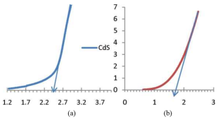
Figure 1. Plot of (Ahv) versus photon energy, hv showing CdS and CoS.
The optical properties of the CdS and CoS thin films were determined using UV-Visible absorption spectrum. Cadmium Sulphide thin film as we see the above plot (Figure 1a) the band gab energy is obtained by extraphlotating the linear portion of (Ahv) versus photon energy (hv) in eV the optical analysis of the energy band gab is around 2.4 eV at PH of 2.5 this showed that the chemical bath is acid bath. This experimental relative similar to the reported review S. thirum avalavan and k. Mani (2015). Who reported optical band gap of Cadmium Sulphide the thin films was found to be 2.40 eV. And also comparative to Isaac Nkrumah2, and Francis Boakyewere reported the energy band gap of CdS was 4.12 eV at pH of 2.35. Here the chemical bath was acidic bath. Evidently our experimental value is appeared between the results of the above reviews. Cobalt Sulphide thin film as we see the above plot (Figure 1b) the band gab energy is obtained by extraphlotating the linear portion of (Ahv) versus photon energy (hv) in eV the optical analysis of the energy band gab is 1.6eV at PH of 6 this showed that the chemical bath is acid bath. this experimental relative similar to the reported review Geetha Govindas, and Priya Murugasen (2016). Who reported optical band gap of cobalt Sulphide the thin films was found to be 1.6 eV. The study of optical properties of CdS thin films has special significance in the world of science, technology and industry for the development of new optical devices. Optical absorption study of materials provides useful information to analyze some features concerning the band structure of materials. The optical band gap energy of the semiconductor is an important parameter that plays a major role in the construction of photovoltaic cells.
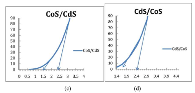
Figure 2. Lot of (Ahv)2 versus photon energy, hv showing hetro structure of CoS/CdS andCdS/CoS.
The optical properties of the CdS /CoS and CoS/ CdS thin films were determined using UV-Visible absorption spectrum. Which have two optical band gaps? As shows Figure 2c UV-V is absorbance of the CoS and CdS thin films grown from a chemical bath at different deposition. The first value is the optical energy band gap is around 1.2 eV and the second is the optical energy band gap 1.6 eV. Then CdS/CoS thin films have low absorbance in the visible region when we compared to pure CdS and the second optical energy band gap relative proportional to pure CoS. The optical properties of the CoS/ CdS thin films were determined using UV-Visible absorption spectrum. In Figure 2d the optical band gap determined two energy band gaps. These values are around 1.1 eV and 1.5 eV respectively. These two results demonstrated that, the two binaries are hetro structure solution since the graph showed the two energy band gap separately. The CoS/CdS thin films have low absorbance in the visible region when we compared to pure CoS.
2.2. Morpohogical Characterization
Scanning Electron Microscope (SEM) is very helpful to study the surface morphology of films. SEM images give information regarding the surface morphology of CdS films show that the films were formed from spherical grains completely covering the substrate without cracks and pinhole (Figure 3e) . The surface of CoS films also covered uniformly without cracks and pinholes with undefined grain shape. When CdS was deposited on CoS to form CdS/CoS heterostructure the surface morphology was changed in such way that cracks were observed and the shape of the grains were not clearly spherical (Figure 3f). Similarly when CoS was deposited on CdS to form CoS/CdS heterostructure, the grains become clearly spherical and some cracks were observed which was not observed when CoS was deposited on glass substrate .
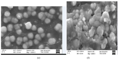
Figure 3. SEM of CoS/CdS and CdS /CoS.
The surface morphological studies of the CoS/ CdS thin films surface was composed of irregular shape changed to spherical shape to have mixed shaped due to CdS affect crack with CoS. when CoS was deposited on CdS to form CoS/CdS heterostructure, the grains become clearly spherical and some cracks were observed which was not observed when CoS was deposited on glass substrate in Figure 3f Similarly When CdS was deposited on CoS to form CdS/CoS heterostructure the surface morphology was changed in such way that cracks were observed and the shape of the grains were not clearly. In CdS/CoS the film is more cracks as comparative to CoS/CdS with surfaces having pinholes. The SEM micrographs showed that the CdS/ CoS thin films surface was composed of spherical shape and this spherical shape changed to irregular have mixed shaped due to CoS affect with cadmium. It also has more cracks. From the micrographs it can be observed that the films exhibited very dense with film surfaces having pinholes. Similar results were reported by Sonawane .The film is very dense with film surfaces having pinholes. The film is composed of many irregular round-shaped grains. The morphology of CdS/CoS structure changes as per deposition method and the preparation parameters like, pH, deposition time, bath temperature, et.
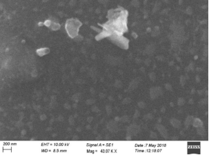
Figure 4. SEM micrographs of CdS.
The SEM image of CoS films deposited on glass substrates at pH 6.it is show that CoS film surface is formed from very compact grain and well uniformly covered. It is also free from crack and pinholes. And also not defined shape it shows is irregular shape without pin hole as it can be observed from Figure 4.
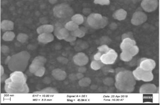
Figure 5. SEM micrographs of CdS.
CdS thin films is spherical shaped grains with different grain sizes and uniformly distributed, From SEM micrographs, it is observed that the films are complex pin hole to each other with the entire area and cover without cracks.
2.3. Structural Characterization
Structural analysis is one of the most common techniques in the characterization of thin films. XRD measurements were carried out to investigate the crystal structure and micro structural parameters of the thin film. The structural characterization heterostructure of CoS and CdS (CdS/CoS) and pure CoS and CdS were determined by Bruker D8 diffract meter with Cukα radiation (lambda=0.15406n. file number 011279). When CdS was deposited on CoS two small peaks were observed at 2 theta value of 26.6 degree which is related to Cubic CdS.
And 45.7 degree which is not related to either CoS or CdS. The grain size of the crystallite is obtained by substituting values of Full Wave Half Maximum (FWHM) in the well-known Debye- Scherer formula.
where D is grain size of the crystallite, K = 0.94, λ (=1.54059 A) is the wavelength of the X-ray source used, β is the broadening of the diffraction line measured at half of its maximum intensity in radians (FWHM) and θ is the angle of diffraction at the peak .
Table 2. Structural parameter of hetro structure CdS, CoS, pure CoS and CdS.

Sample

Standard values 2θ(deg)

hkl value

FWHM

2θ(deg)

Observed intensity

Crystalline Size D(nm)

CoS

19.465

1 1 1

0.11307

20.41675

1213.9504

71.4

22.478

2 0 0

0.11884

21,64609

326.78798

68

32.228

2 2 0

0.12604

22.24599

584.83516

63

37.858

3 1 1

8.94584

24.04519

108.35441

0.9

39.509

2 2 2

230956.39872

30.7752

34.92437

45.825

4 0 0

50.235

3 3 0

45.825

4 0 0

CdS

26.547

1 11

2.2760

26.70272

69.46205

3.4

C0S/CdS

1 1 1

0.26872

26.7937

2083.02523

30.3

CdS/CoS

2 0 0

0.42232

21.40356

103.81718

19

230.93464

21.40356

26.9623

0.03

0.17769

26.53429

108.35278

74.6

0.27451

26.7085

147.84766

29.8

68.5608

26.785

39.95526

0.1

4 0 0

0.2004

45.74755

165.65453

43

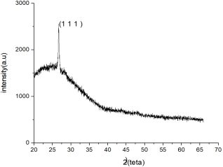
Figure 6. XRD pattern for pure CdS.
XRD pattern of CdS films show a single sharp peak at 2 theta value of 26 degree (Figure 6) which was indexed to (111) plane of cubic CdS comparing with JCPDS file number 01-080 0019.
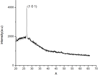
Figure 7. XRD pattern for heterostructure CoS / CdS.
The crystallinity of the films CoS/CdS, is good and characterized by, one principal peaks at 2θ values of approximately 26, which are indexed to (1 0 1), the diffraction pattern was well relatively with standard JCPDS data file reference code: 01-080-001. This is a typical characteristic observation of a face centered cubic structure.
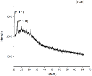
Figure 8. XRD pattern for heterostructure CoS.
The XRD patterns of CoS are The crystallinity of the films is good and characterized by two principal peaks at 2θ values of approximately 20, 21. 20 and 45 which are indexed to (1 1 1), (22 0), respectively. The diffraction pattern was well relatively with standard JCPDS data file reference code: 1.9373.This is a typical characteristic observation of a face centered cubic structure.
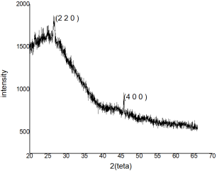
Figure 9. XRD pattern for heterostructure CdS / CoS.
The figure above shows the XRD patterns of CdS/CoS are The crystallinity of the films is good and characterized by two principal peaks at 2θ values of approximately 20, 21. 20 and 45 which are indexed to (2 2 0) and (4 0 0) respectively. The diffraction pattern was well relatively with standard JCPDS data file reference code: 1.9373.This is a typical characteristic observation of a face centered cubic structure.
2.4. EDX Analysis of the Films
Chemical Composition Studies of the hetro structure CdS and CoS Thin Films. Elemental analyses of the hetro structure thin films were carried out by using the EDX (Energy-Dispersive X-ray) technique to study the stoichiometry of the films. The elemental analysis was carried out only for CdS, S, and Co element e energy dispersive X-ray (EDX) data of the films were taken. EDX result reveals that the deposited films are very close to the nominal composition. From Figure 9, it is observed that the emission lines of Cd and S are present in the EDX spectra indicating the formation of CdS thin films. The EDX spectrum of the deposited CdS thin films, which is consistent with the formation of the binary compound. The atomic percentage of Cd:S is 48:52 at pure CdS, which is nearly 1:1 indicating that the thin film had the desired stoichiometric ratio and also the atomic percentage of Cd:S: Co thin film were 26.7:66.06:7.22, respectively. The results indicate that an excess of sulphur was observed for all the thin films. The presence of carbon, sodium, magnesium, silicon, calcium and sulfur may be the composition of glass substrate used for deposition of thin films.
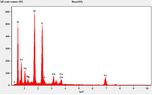
Figure 10. EDX spectrum of CoS /CdS thin films deposion.
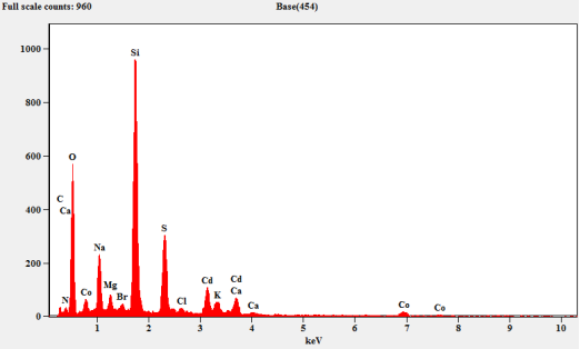
Figure 11. EDX spectrum of CdS /CoS thin films.
Chemical Composition Studies of the hetro structure CdS / CoS Thin Films. Elemental analyses of the hetro structure thin films were carried out by using the EDX (Energy-Dispersive X-ray) technique to study the stoichiometry of the films. The elemental analysis was carried out only for CdS, S, and Co element e energy dispersive X-ray (EDX) data of the films were taken. EDX result reveals that the deposited films are very close to the nominal composition.
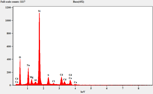
Figure 12. EDX spectrum of CdS thin films.
The EDX spectrum of the deposited CdS thin films, which is consistent with the formation of the binary compound. The atomic percentage of Cd:S is 48:52 at pure CdS, which is nearly 1:1 indicating that the thin film had the desired stoichiometric ratio and also the atomic percentage of Cd:S: Co thin film were 26.7:66.06:7.22, respectively. The results indicate that an excess of sulphur was observed for all the thin films. The presence of carbon, sodium, magnesium, silicon, calcium and sulfur may be the composition of glass substrate used for deposition of thin film.
3. Discussion
1.6 eV. Geetha Govindas and Priya Murugasen (2016) has reported 1.6 eV band gap for CoS thin films. The band gap of CdS/CoS is shown in Figure 2b. This heterostructure has two band gaps for CdS (2.4eV) and CoS (1.65eV). Similarly the CoS/CdS has two band gaps for CoS (1.45 eV) and CdS (2.5eV) as shown in Figure 2a. The surface of CoS films also covered uniformly without cracks and pinholes with undefined grain shape (Figure 1a). When CdS was deposited on CoS to form CdS/CoS heterostructure the surface morphology was changed in such way that cracks and some cracks were observed which was not observed when CoS was deposited on glass substrate (Figure 3a) were observed and the shape of the grains were not clearly spherical (Figure 3b). Similarly when CoS was deposited on CdS to form CoS/CdS heterostructure, the grains become clearly spherical.
4. Conclusion
The CdS and CoS thin films and their heterostructure were produced successfully by chemical bath deposition under acidic conditions. Optical measurements gave band gaps of about 2.4 eV for CdS and 1.6 eV for CoS, and the CdS/CoS and CoS/CdS junctions exhibited two distinct band-gap features corresponding to each constituent. SEM imaging showed that CoS formed a dense, continuous coating, while the heterostructure films consisted of well-dispersed, roughly spherical grains of varying sizes; the CdS/CoS stacks in particular were compact but contained a few small pinhole-like cracks. XRD patterns identified a cubic phase for CdS and for the CoS/CdS sample, a hexagonal phase for CoS, and a mixture of both crystal systems in the CdS/CoS configuration, with the dominant cubic reflection indexed to the (111) plane. EDX confirmed the expected stoichiometry of CdS and detected Cd, Co and S in the heterostructure. Overall, these results indicate that substrate choice substantially influences the films’ structural, optical and morphological properties.
5. Recommendation
As this study explores a rarely reported fabrication method for CdS/CoS heterostructure, several paths for future work are suggested: Morphological Optimization: Research should be conducted to minimize surface defects and pinholes identified in the CdS/CoS stacks to improve film quality. Performance Testing: Future projects should move beyond structural characterization to test the electrical properties and photo-conversion efficiency of these heterostructure in solar cells. Environmental Stability: Investigating the long-term stability of these thin films under various environmental conditions will be crucial for their industrial application.
Abbreviations

CoS

Cobalt Sulfide

CdS

Cadmium Sulfide

CoS/CdS

Cobalt Sulfide over Cadmium Sulfide

CdS/CoS

Cadmium Sulfide over Cobalt Sulfide

CBD

Chemical Bath Deposition

XRD

X-ray Diffraction

SEM

Scanning Electron Microscopy

UV-V

UV-Visible Spectroscopy

EDX

Energy-Dispersive X-ray Spectroscopy

Acknowledgments
I want to express our gratitude to our family and everyone else who assisted make this study possible, both directly and indirect.
Author Contributions
Tangut Masreshaw Eshete: Project administration, methodology.
Takele Teshome Somano: Conceptualization, Formal Analysis.
Data Availability Statement
The XRD, UV-VIS, FTIR and EDX data used to support the findings of this study are available.
Conflicts of Interest
The author declares no conflicts of interest regarding the publication of this paper.
References
[1] O. Calzadilla, F. Chale-lara, V. Rejonc, J.L. Pena, F. Caballero-Brionesa, "Mg-doped CdS films prepared by chemical bath deposition. optical," Chalcogenide Letters, April 2015 vol. 12, no. 4, p. 137 – 145.
[2] K.mani, S. sagadevan, S.thirumavalavan, "Studies on Structural," Journal of Ovonic Research, 2015., vol. 11, no. 5, p. 203 – 211.
[3] Hadi Ahmed Hussin, "Urbach energy and dispersion parameters of CdSchemically deposited thin films on the effect of thickness," international scientific journal 2018. pp. 241-249.
[4] Ahmed N. Abd, "Improved Photoresponse of Porous Silicon Photodetectors by EmbeddingImproved Photoresponse of Porous Silicon Photodetectors by Embedding," 2016. J. Nano. Adv. Mat., vol. 4, no. 1, pp. 33-44, 1.
[5] R.Hepzi Pramila Devamani, "Synthesis and Characterization of Cadmium Sulfide Nanoparticles," International Journal of Innovative Science, Engineering & Technology,, January 2017, vol. 4, no. 1.
[6] Robabe Mohammadzadeh-Hesar, Shahin Khademinia Leila Kafi-Ahmadi, "Influence of reactionparameters on crystal phase growth and optical properties of ultrasonic assisted Hydro-and solvothermal synthesized sub-micrometer-sized CdSspheres," Int. J. Nano Dimens. 2018., 9, vol. 9, no. 4, pp. 346-356.
[7] A. a. azizova, m. b. muradov, a. m. maharramov, g. m.eyvazova o. o. balayeva, "synthesis and characterization of cobalt sulfide/fnbrnanocomposites by silar method," journal of ovonic research november - 2016. vol. 12, no. 6, pp. 267 - 273, november - 2016.
[8] Ofeliya O. Balayeva, Abdulsaid A. Azizova, Abel M. Maharramova, Lala R. Qahramanlib, Goncha M. Eyvazovab, Zohrab A. Aghamaliyevb Mustafa B. Muradovb, "Synthesis and characterization of cobalt sulfide nanoparticles by sonochemical method," ScienceDirect, june 2018.
[9] M. S sonawane, R. spatill characterization of chemical deposited nano crystalline cobalt sulphide thin film. 3 2014.
[10] Tizazu, A., et al., A New Route for the S. nthesis of CdS Thin Films from Acidic Chemical Baths. Int. J. Thin. Film Sci. Tec, 2017. 6(2): p. 67-71.
[11] Mane, S., S. Kamble, and L. Deshmukh, Cobalt sulphide thin films: Chemical bath deposition, growth and properties. Materials Letters, 2011. 65(17-18): p. 2639-2641.
[12] Markus Neuwirtha, Elisabeth Seydela, Jasmin Seeger, Alexander Welle Heinz Kalt, Michael Hetterich, B, "h, Band-gap tuning of Cu2ZnSn(S,Se)4 solar cell absorbers via definedincorporation of sulphur based on a post-sulphurization process," ScienceDirect 2018., pp. 158-165.
[13] Francis Kofi Ampong, Fekadu Gashaw Hone, Robert Kwame Nkum, Francis Boaky Tizazu Abzaa, "Preparation of cadmium zinc sulfide (Cd1-xZnxS) thin films from acidic chemicalBAS,", ScienceDirect, 2018. no. 66, pp. 28-33.
[14] K. Rajathi and A. Rajendran, "n Green Synthesis of Stable CdSNanoparticlesfrom Imidazolium Ionic Liquids and their Antibacterial Activities," Global Research Publications, January-March 2015.vol. 10, no. 1, pp. 1-8.
[15] Andrzej Sikora, S.T. Pawar, N.N. Maldar, L.P. Deshmukh P A 5S.S. Kamble, "1 Cobalt sulfide thin films: Chemical growth, reaction kinetics and microstructuralanalyis,", ScienceDirect 2015., no. 623, p. 466-472.
[16] Jose Luis G. Fierro and Rufino M. Navarro Yerga, Fernando Vaquero, "Nanowires of CdS Synthesized by a Solvothermal Method: Influence of the Morphologyon the Photoactivity for Hydrogen Evolution from Water," MDPI, March 2016 no. 24.
[17] K. Manikandan, C. Surendra Dilip, P. Mani and J. Joseph Prince, 7, "Deposition and Characterization of CdS Nano Thin Film with Complexing Agent Triethanolamine," American journal oe Egnering and Applied science, 2015.
[18] Rajeshwar Sharma, Raghvendra Singh Yadav, Diwakar Kashyap, S. L. Kothari S. Kachhwaha Aryan Sankhla, "a, Biosynthesis and characterization of cadmium sulfidenanoparticles e An emphasis of zeta potential behavior due to capping", ScienceDirect, 2015.pp. 1-8.
[19] Gebremeskel Tekle, Eyobe Belew Abebe, and Kalid Seid Ahmed Tizazu Abza, "Characterization of Cobalt Sulfide Thin Films Synthesized from Acidic Chemical BAS," Hindawi.
Cite This Article
  • APA Style

    Eshete, T. M., Somano, T. T. (2026). Synthesis and Characterization of Cadmium Sulphide (CdS) and Cobalt Sulphide (CoS) Heterostructure Using the Chemical Bath Deposition Method. American Journal of Chemical Engineering, 14(1), 8-18. https://doi.org/10.11648/j.ajche.20261401.12

    Copy | Download

    ACS Style

    Eshete, T. M.; Somano, T. T. Synthesis and Characterization of Cadmium Sulphide (CdS) and Cobalt Sulphide (CoS) Heterostructure Using the Chemical Bath Deposition Method. Am. J. Chem. Eng. 2026, 14(1), 8-18. doi: 10.11648/j.ajche.20261401.12

    Copy | Download

    AMA Style

    Eshete TM, Somano TT. Synthesis and Characterization of Cadmium Sulphide (CdS) and Cobalt Sulphide (CoS) Heterostructure Using the Chemical Bath Deposition Method. Am J Chem Eng. 2026;14(1):8-18. doi: 10.11648/j.ajche.20261401.12

    Copy | Download

  • @article{10.11648/j.ajche.20261401.12,
      author = {Tangut Masreshaw Eshete and Takele Teshome Somano},
      title = {Synthesis and Characterization of Cadmium Sulphide (CdS) and Cobalt Sulphide (CoS) Heterostructure Using the Chemical Bath Deposition Method},
      journal = {American Journal of Chemical Engineering},
      volume = {14},
      number = {1},
      pages = {8-18},
      doi = {10.11648/j.ajche.20261401.12},
      url = {https://doi.org/10.11648/j.ajche.20261401.12},
      eprint = {https://article.sciencepublishinggroup.com/pdf/10.11648.j.ajche.20261401.12},
      abstract = {In this study, cadmium Sulphide (CdS), a group II–VI semiconductor known for its wide applications in optoelectronics, piezoelectric devices, and other semiconductor technologies, and cobalt Sulphide (CoS), notable for its roles in solar-selective coatings, infrared sensing, and photo electrochemical energy storage, were investigated. Thin films of CdS, CoS, and their heterostructure (CdS/CoS and CoS/CdS) were synthesized via the chemical bath deposition (CBD) method at 80°C for 1.5 hours, using cadmium acetate, cobalt acetate, thioacetamide, and EDTA as precursor materials. The films were characterized using X-ray diffraction (XRD), scanning electron microscopy (SEM), energy-dispersive X-ray spectroscopy (EDX), and optical absorption spectroscopy. Optical measurements revealed that pure CdS and CoS films exhibited direct band gaps of 2.4 eV and 1.6 eV, respectively, at deposition pH values of 2.5 and 6. The heterostructure films showed dual band gaps of 2.4 eV (CdS) and 1.65 eV (CoS) for CdS/CoS, and 1.45 eV (CoS) and 2.5 eV (CdS) for CoS/CdS. SEM analyses indicated that CoS films were compact with uniformly distributed grains, while CdS films displayed smooth, spherical grains free of pinholes. The CdS/CoS layers appeared denser with occasional surface defects. XRD analysis confirmed that CdS and CoS/CdS films crystallized in a cubic structure with a preferred (111) orientation, CoS exhibited a hexagonal phase, and CdS/CoS composites displayed a mixed cubic–hexagonal structure. EDX results showed a near-stoichiometric Cd/S ratio (48:52) in CdS and validated the presence of Cd, Co, and S in all prepared samples.},
     year = {2026}
    }
    

    Copy | Download

  • TY  - JOUR
    T1  - Synthesis and Characterization of Cadmium Sulphide (CdS) and Cobalt Sulphide (CoS) Heterostructure Using the Chemical Bath Deposition Method
    AU  - Tangut Masreshaw Eshete
    AU  - Takele Teshome Somano
    Y1  - 2026/02/06
    PY  - 2026
    N1  - https://doi.org/10.11648/j.ajche.20261401.12
    DO  - 10.11648/j.ajche.20261401.12
    T2  - American Journal of Chemical Engineering
    JF  - American Journal of Chemical Engineering
    JO  - American Journal of Chemical Engineering
    SP  - 8
    EP  - 18
    PB  - Science Publishing Group
    SN  - 2330-8613
    UR  - https://doi.org/10.11648/j.ajche.20261401.12
    AB  - In this study, cadmium Sulphide (CdS), a group II–VI semiconductor known for its wide applications in optoelectronics, piezoelectric devices, and other semiconductor technologies, and cobalt Sulphide (CoS), notable for its roles in solar-selective coatings, infrared sensing, and photo electrochemical energy storage, were investigated. Thin films of CdS, CoS, and their heterostructure (CdS/CoS and CoS/CdS) were synthesized via the chemical bath deposition (CBD) method at 80°C for 1.5 hours, using cadmium acetate, cobalt acetate, thioacetamide, and EDTA as precursor materials. The films were characterized using X-ray diffraction (XRD), scanning electron microscopy (SEM), energy-dispersive X-ray spectroscopy (EDX), and optical absorption spectroscopy. Optical measurements revealed that pure CdS and CoS films exhibited direct band gaps of 2.4 eV and 1.6 eV, respectively, at deposition pH values of 2.5 and 6. The heterostructure films showed dual band gaps of 2.4 eV (CdS) and 1.65 eV (CoS) for CdS/CoS, and 1.45 eV (CoS) and 2.5 eV (CdS) for CoS/CdS. SEM analyses indicated that CoS films were compact with uniformly distributed grains, while CdS films displayed smooth, spherical grains free of pinholes. The CdS/CoS layers appeared denser with occasional surface defects. XRD analysis confirmed that CdS and CoS/CdS films crystallized in a cubic structure with a preferred (111) orientation, CoS exhibited a hexagonal phase, and CdS/CoS composites displayed a mixed cubic–hexagonal structure. EDX results showed a near-stoichiometric Cd/S ratio (48:52) in CdS and validated the presence of Cd, Co, and S in all prepared samples.
    VL  - 14
    IS  - 1
    ER  - 

    Copy | Download

Author Information